- 您现在的位置:买卖IC网 > Sheet目录1222 > ISL62386HIEVAL1Z (Intersil)EVAL BOARD FOR ISL62386HI 32TQFN
�� �
�
�ISL62386�
�V� OUT� =� V� REF� ?� ?� ?�
�flows� out� of� the� ISEN1� pin,� generating� a� voltage� drop� on� the�
�R� O� resistor,� which� should� be� chosen� to� have� the� same�
�resistance� as� R� OCSET� .� When� PGOOD� pin� goes� high,� the�
�ISEN1� pin� current� source� will� be� removed.�
�When� an� OCP� fault� is� detected� in� one� SMPS� channel,� the�
�PGOOD� pin� will� pull� down� to� 32� Ω� .� The� ISL62386� turns� the�
�faulted� channel� UGATE� and� LGATE� off� and� latches� off� the�
�faulted� channel.�
�The� fault� will� remain� latched� until� either� of� the� EN� pins� has�
�been� pulled� below� the� falling� EN� threshold� voltage,� or� until�
�V� IN� has� decayed� below� the� falling� POR� threshold.�
�When� using� a� discrete� current� sense� resistor,� inductor�
�time-constant� matching� is� not� required.� Equation� 7� remains�
�unchanged,� but� Equation� 8� is� modified� in� Equation� 11:�
�Programming� the� Output� Voltage�
�When� the� converter� is� in� regulation� there� will� be� 0.6V�
�between� the� FB� and� GND� pins.� Connect� a� two-resistor�
�voltage� divider� across� the� OUT� and� GND� pins� with� the�
�output� node� connected� to� the� FB� pin� as� shown� in� Figure� 27.�
�Scale� the� voltage-divider� network� such� that� the� FB� pin� is�
�0.6V� with� respect� to� the� GND� pin� when� the� converter� is�
�regulating� at� the� desired� output� voltage.� The� output� voltage�
�can� be� programmed� from� 0.6V� to� 5.5V.�
�Programming� the� output� voltage� is� written� as� Equation� 13:�
�?� R� TOP� ?�
�1� +� -----------------------------� (EQ.� 13)�
�?� R� BOTTOM� ?�
�Where:�
�-� V� OUT� is� the� desired� output� voltage� of� the� converter�
�R� OCSET� =� -------------------------------------�
�V� OCSET1� –� V� ISEN1� =� I� L� ?� R� SENSE� –� 10� μ� A� ?� R� OCSET�
�Furthermore,� Equation� 9� is� changed� in� Equation� 12:�
�I� OC� ?� R� SENSE�
�10� μ� A�
�(EQ.� 11)�
�(EQ.� 12)�
�-� The� voltage� to� which� the� converter� regulates� the� FB� pin�
�is� the� V� REF� (0.6V)�
�-� R� TOP� is� the� voltage-programming� resistor� that� connects�
�from� the� FB� pin� to� the� converter� output.� In� addition� to�
�setting� the� output� voltage,� this� resistor� is� part� of� the� loop�
�compensation� network�
�Where� R� SENSE� is� the� series� power� resistor� for� sensing�
�inductor� current.� For� example,� with� an� R� SENSE� =� 1m� Ω� and�
�an� OCP� target� of� 10A,� R� OCSET� =� 1k� Ω.�
�Overvoltage� Protection�
�-� R� BOTTOM� is� the� voltage-programming� resistor� that�
�connects� from� the� FB� pin� to� the� GND� pin�
�Choose� R� TOP� first� when� compensating� the� control� loop,� and�
�then� calculate� R� BOTTOM� according� to� Equation� 14:�
�R� BOTTOM� =� -------------------------------------�
�The� OVP� fault� detection� circuit� triggers� after� the� FB� pin�
�voltage� is� above� the� rising� overvoltage� threshold� for� more�
�than� 2μs.� The� FB� pin� voltage� is� 0.6V� in� normal� operation.�
�V� REF� ?� R� TOP�
�V� OUT� –� V� REF�
�(EQ.� 14)�
�The� rising� overvoltage� threshold� is� typically� 116%� of� that�
�value,� or� 1.16*0.6V� =� 0.696V.�
�If� an� OVP� is� detected� in� one� SMPS� channel,� the� PGOOD� pin�
�will� pull-down� to� 32� Ω,� and� the� LGATE� gate-driver� will� turn� on�
�the� low-side� MOSFET� to� discharge� the� output� voltage,� thus�
�protecting� the� load� from� potentially� damaging� voltage� levels.�
�Once� the� FB� pin� voltage� falls� to� 106%� of� the� reference�
�voltage,� or� 1.06*0.6V� =� 0.636V,� the� faulted� channel� will�
�resume� the� normal� switching,� and� PGOOD� will� go� high� when�
�Compensation� Design�
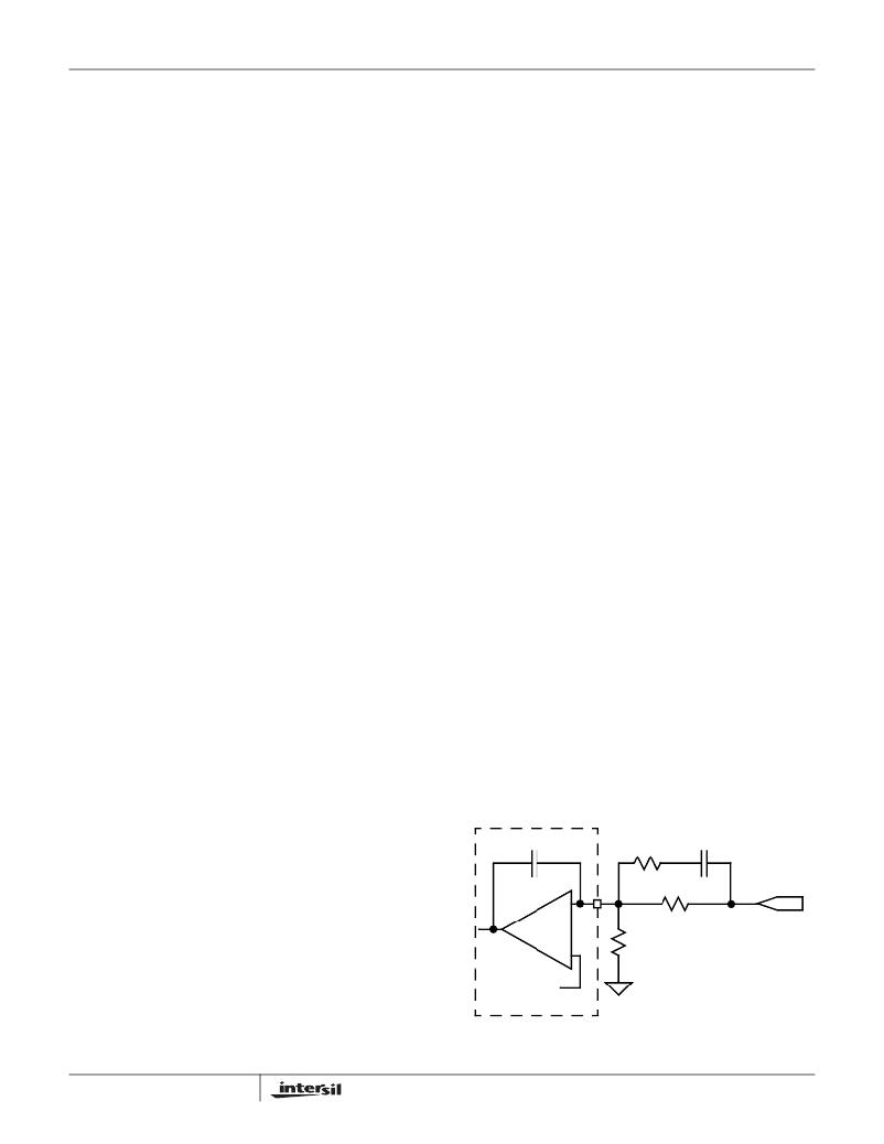
�Figure� 27� shows� the� recommended� Type-II� compensation�
�circuit.� The� FB� pin� is� the� inverting� input� of� the� error� amplifier.�
�The� COMP� signal,� the� output� of� the� error� amplifier,� is� inside� the�
�chip� and� unavailable� to� users.� C� INT� is� a� 100pF� capacitor�
�integrated� inside� the� IC� that� connects� across� the� FB� pin� and� the�
�COMP� signal.� R� TOP� ,� R� FB� ,� C� FB� and� C� INT� form� the� Type-II�
�compensator.� The� frequency� domain� transfer� function� is� given�
�by� Equation15:�
�s� ?� R� TOP� ?� C� INT� ?� (� 1� +� s� ?� R� FB� ?� C�
�the� output� voltage� is� in� regulation.� This� process� repeats� as�
�long� as� the� OVP� fault� is� present.�
�Undervoltage� Protection�
�1� +� s� ?� (� R� TOP� +� R� FB� )� ?� C� FB�
�)�
�G� COMP� (� s� )� =� -------------------------------------------------------------------------------------------�
�FB�
�(EQ.� 15)�
�The� UVP� fault� detection� circuit� triggers� after� the� FB� pin�
�C� INT� =� 100pF�
�R� FB�
�C� FB�
�voltage� is� below� the� undervoltage� threshold� for� more� than�
�2μs.� The� undervoltage� threshold� is� typically� 86%� of� the�
�reference� voltage,� or� 0.86*0.6V� =� 0.516V.�
�-�
�FB�
�R� TOP�
�VO�
�If� a� UVP� fault� is� detected� in� one� SMPS� channel,� the� PGOOD�
�EA�
�pin� will� pull-down� to� 32� Ω� .� The� ISL62386� turns� the� faulted�
�COMP�
�R� BOTTOM�
�channel� UGATE� and� LGATE� off� and� latches� off� the� faulted�
�channel.�
�The� fault� will� remain� latched� until� either� of� the� EN� pins� has�
�been� pulled� below� the� falling� EN� threshold� voltage,� or� until�
�VIN� has� decayed� below� the� falling� POR� threshold.�
�15�
�+�
�REF�
�ISL62386�
�FIGURE� 27.� COMPENSATION� REFERENCE� CIRCUIT�
�FN6831.0�
�February� 4,� 2009�
�发布紧急采购,3分钟左右您将得到回复。
相关PDF资料
ISL6291EVAL1
EVALUATION BOARD FOR ISL6291
ISL6292EVAL2
EVALUATION BOARD 2 ISL6292
ISL6296EVAL1
EVALUATION BOARD 1 ISL6296
ISL6298EVAL1
EVALUATION BOARD 1 ISL6298
ISL6298EVAL2
EVALUATION BOARD 2 ISL6298
ISL6299AEVAL1
EVALUATION BOARD 1 ISL6299A
ISL6411EVAL1
EVALUATION BOARD ISL6411
ISL6413EVAL1
EVALUATION BOARD ISL6413
相关代理商/技术参数
ISL62386HRTZ
功能描述:IC PWR SUPPLY CTRLR QUAD 32TQFN RoHS:是 类别:集成电路 (IC) >> PMIC - 电源控制器,监视器 系列:- 产品培训模块:Lead (SnPb) Finish for COTS
Obsolescence Mitigation Program 标准包装:2,500 系列:- 应用:多相控制器 输入电压:- 电源电压:9 V ~ 14 V 电流 - 电源:- 工作温度:-40°C ~ 85°C 安装类型:表面贴装 封装/外壳:40-WFQFN 裸露焊盘 供应商设备封装:40-TQFN-EP(5x5) 包装:带卷 (TR)
ISL62386HRTZ-T
功能描述:IC PWR SUPPLY CTRLR QUAD 32TQFN RoHS:是 类别:集成电路 (IC) >> PMIC - 电源控制器,监视器 系列:- 产品培训模块:Lead (SnPb) Finish for COTS
Obsolescence Mitigation Program 标准包装:2,500 系列:- 应用:多相控制器 输入电压:- 电源电压:9 V ~ 14 V 电流 - 电源:- 工作温度:-40°C ~ 85°C 安装类型:表面贴装 封装/外壳:40-WFQFN 裸露焊盘 供应商设备封装:40-TQFN-EP(5x5) 包装:带卷 (TR)
ISL62386LOEVAL1Z
功能描述:EVAL BOARD FOR ISL62386LO 32TQFN RoHS:是 类别:编程器,开发系统 >> 评估演示板和套件 系列:* 标准包装:1 系列:PCI Express® (PCIe) 主要目的:接口,收发器,PCI Express 嵌入式:- 已用 IC / 零件:DS80PCI800 主要属性:- 次要属性:- 已供物品:板
ISL62391
制造商:INTERSIL 制造商全称:Intersil Corporation 功能描述:High-Efficiency, Triple-Output System Power Supply Controller
ISL62391_11
制造商:INTERSIL 制造商全称:Intersil Corporation 功能描述:High-Efficiency, Triple-Output System Power Supply Controller
ISL62391CHRTZ
功能描述:IC PWR SUPPLY CTRLR 28TQFN RoHS:是 类别:集成电路 (IC) >> PMIC - 电源控制器,监视器 系列:- 产品培训模块:Lead (SnPb) Finish for COTS
Obsolescence Mitigation Program 标准包装:2,500 系列:- 应用:多相控制器 输入电压:- 电源电压:9 V ~ 14 V 电流 - 电源:- 工作温度:-40°C ~ 85°C 安装类型:表面贴装 封装/外壳:40-WFQFN 裸露焊盘 供应商设备封装:40-TQFN-EP(5x5) 包装:带卷 (TR)
ISL62391CHRTZ-T
功能描述:IC PWR SUPPLY CTRLR 28TQFN RoHS:是 类别:集成电路 (IC) >> PMIC - 电源控制器,监视器 系列:- 产品培训模块:Lead (SnPb) Finish for COTS
Obsolescence Mitigation Program 标准包装:2,500 系列:- 应用:多相控制器 输入电压:- 电源电压:9 V ~ 14 V 电流 - 电源:- 工作温度:-40°C ~ 85°C 安装类型:表面贴装 封装/外壳:40-WFQFN 裸露焊盘 供应商设备封装:40-TQFN-EP(5x5) 包装:带卷 (TR)
ISL62391CIRTZ
功能描述:IC PWR SUPPLY CTRLR 28TQFN RoHS:是 类别:集成电路 (IC) >> PMIC - 电源控制器,监视器 系列:* 产品培训模块:Lead (SnPb) Finish for COTS
Obsolescence Mitigation Program 标准包装:2,500 系列:- 应用:多相控制器 输入电压:- 电源电压:9 V ~ 14 V 电流 - 电源:- 工作温度:-40°C ~ 85°C 安装类型:表面贴装 封装/外壳:40-WFQFN 裸露焊盘 供应商设备封装:40-TQFN-EP(5x5) 包装:带卷 (TR)